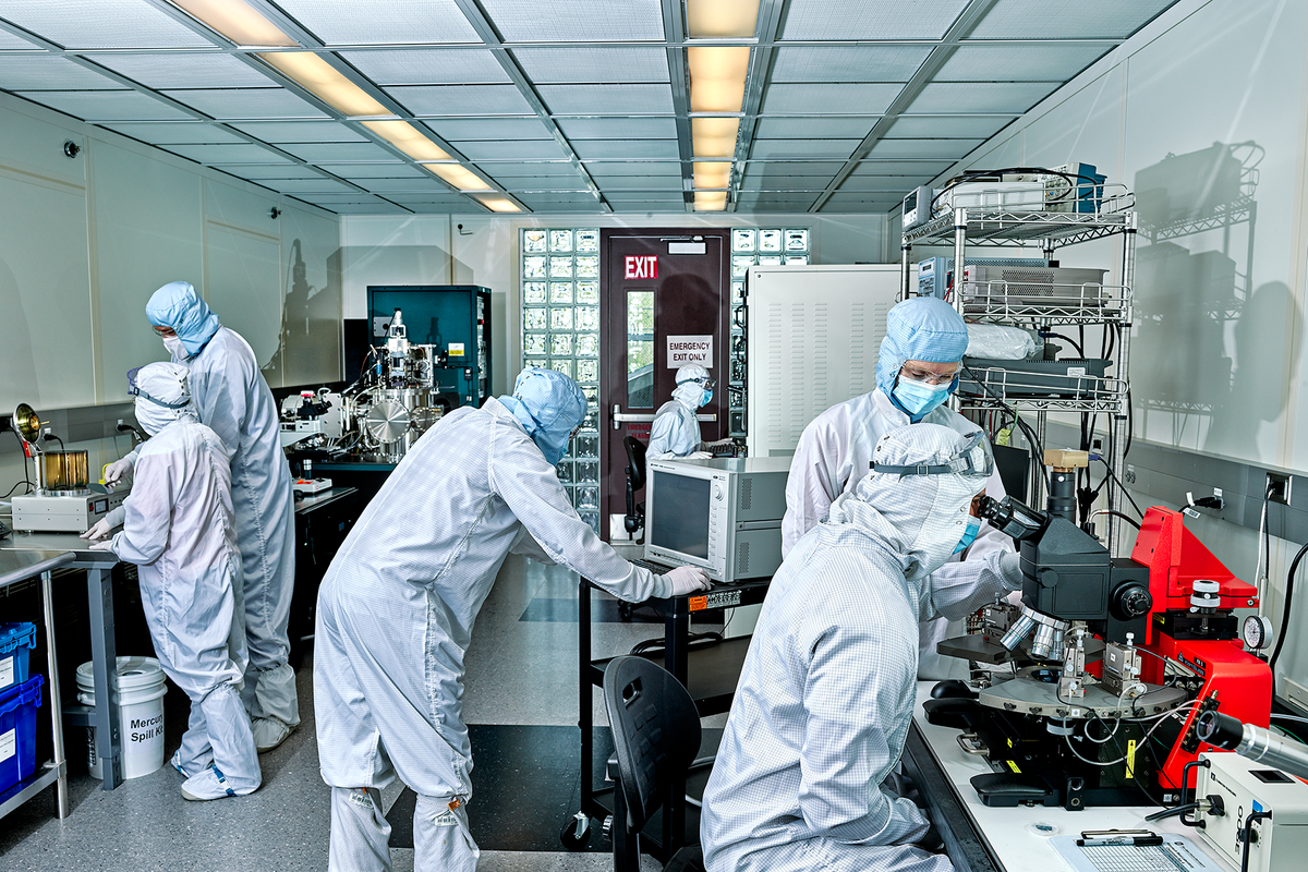
The CHIPS and Science Act, aimed at kick-starting chip manufacturing in the United States, only began taking requests for pieces of its US $50 billion in March, but chipmakers were already gearing up beforehand. Memory and storage chipmaker Micron announced as much as $100 billion for a new plant in upstate New York. Taiwan Semiconductor Manufacturing Co. (TSMC), which was already building a $12 billion fab in Arizona, upped the investment to $40 billion with a second plant. Samsung is planning a $17 billion fab near Austin, Texas, and in September Intel broke ground on the first of two massive new facilities worth $20 billion in central Ohio.
Exciting as this is for the U.S. economy, there’s a potential problem: Where will the industry find the qualified workforce needed to run these plants and design the chips they’ll make? The United States today manufactures just 12 percent of the world’s chips, down from 37 percent in 1990, according to a September 2020 report by the Semiconductor Industry Association. Over those decades, experts say, semiconductor and hardware education has stagnated. But for the CHIPS Act to succeed, each fab will need hundreds of skilled engineers and technicians of all stripes, with training ranging from two-year associate degrees to Ph.D.s.
Engineering schools in the United States are now racing to produce that talent. Universities and community colleges are revamping their semiconductor-related curricula and forging strategic partnerships with one another and with industry to train the staff needed to run U.S. foundries. There were around 20,000 job openings in the semiconductor industry at the end of 2022, according to Peter Bermel, an electrical and computer engineering professor at Purdue University. “Even if there’s limited growth in this field, you’d need a minimum of 50,000 more hires in the next five years. We need to ramp up our efforts really quickly.”
Intel arrives at Ohio State
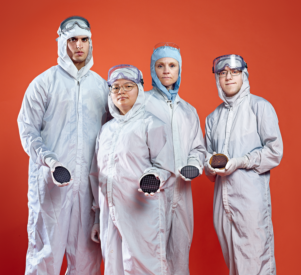 Ohio State University is using its chip-fabrication facility to train future engineers and technicians. Here, from left to right, are OSU students Caleb Mallory and Jayne Griffith, manager of nanofabrication Aimee Price, and Columbus State Community College student Chris Staudt, who’s also on staff at OSU’s Nanotech West Laboratory.Peter Adams
The U.S. Midwest might be known more for farming and heavy industry than semiconductors, but chipmakers are betting it is fertile ground for their industry, thanks to an abundance of research universities and technical colleges.
Take Intel, which wants to create a “Silicon Heartland” in Ohio. In addition to building two cutting-edge chip factories on a 4-square-kilometer megasite that could hold six more fabs, the company has pledged $50 million to 80 higher-education institutions in the state. The funds should help the universities and community colleges upgrade their curricula, train and hire faculty, and provide equipment, and Intel also plans to provide internships, guidance, and research opportunities.
Part of those funds have gone to Ohio State University, which will lead a new interdisciplinary Center for Advanced Semiconductor Fabrication Research and Education that will span 10 in-state colleges and universities. While most of the semiconductor-related curriculum has been designed for students in electrical and computer engineering, OSU now wants to bring in students from other disciplines. The university is creating tracks for them to master semiconductor-related skills, and it’s revamping the curriculum in those disciplines to reflect the latest industry technology. Materials engineers will have new courses on chip packaging materials, industrial system engineers will learn semiconductor manufacturing processes, and mechanical engineers will get to know device fabrication tools, says Ayanna Howard, dean of OSU’s college of engineering. “Now that we’re bringing manufacturing back to [U.S.] shores, our curriculum is now bringing in all these components that have always been needed but haven’t been part of the plan at the scale required to train all these engineers.”
There is no shortage of talent in the region, Howard adds, since manufacturing is already a major activity in Ohio and other parts of the Midwest. In 2011, Ohio kicked off an initiative called Jobs Ohio to create more science, technology, engineering, and medicine (STEM) graduates in the areas of computer science, biotech, and health-care manufacturing. It’s now a matter of overhauling the curricula to cater to semiconductor manufacturing, she says. “When Intel came to the region, it really reinforced all the things that we had been thinking about.”
In addition to leading two projects with state colleges, OSU is collaborating with 10 other midwestern institutions, including Purdue and the University of Michigan, to “think about engineering education more holistically,” says Howard. “How do we create a curriculum that allows universities that might not have the infrastructure—say, lab space or trained faculty—to give students semiconductor experience?”
In the fall of 2021, for example, OSU piloted a course to teach students about chip-fabrication processes using desktop laboratory equipment, allowing them to learn without an expensive clean room. The engineering school is also teaming up with the creative arts department to create augmented-reality and virtual-reality tools that will let students experience a simulated fab.
SkyWater moves next door to Purdue
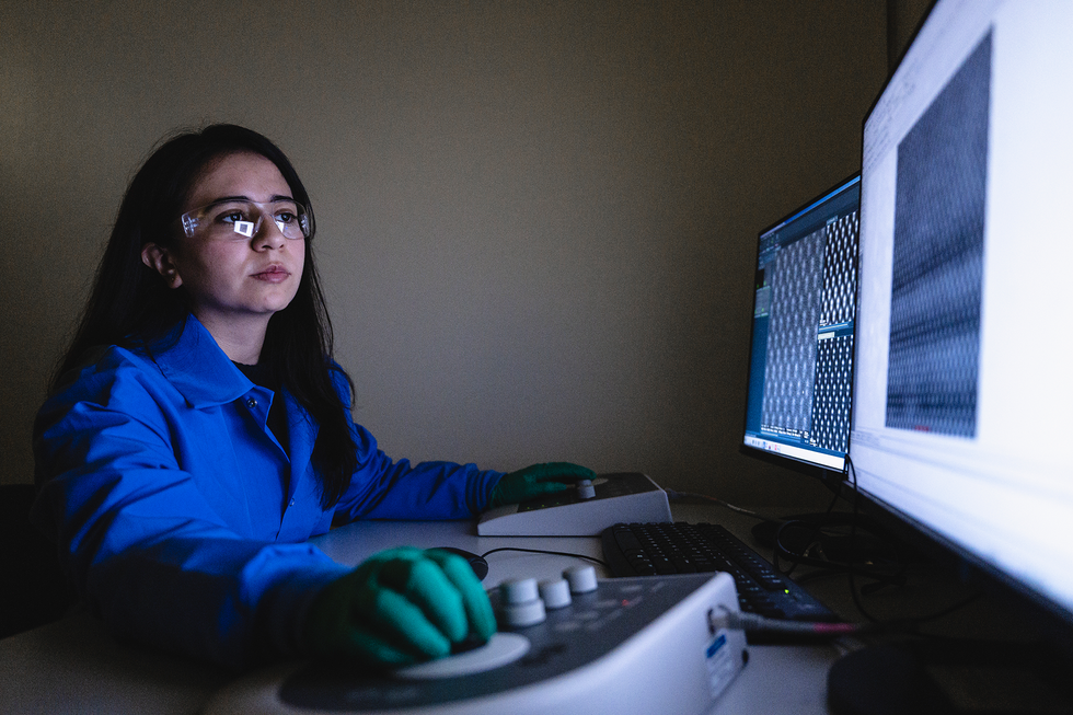
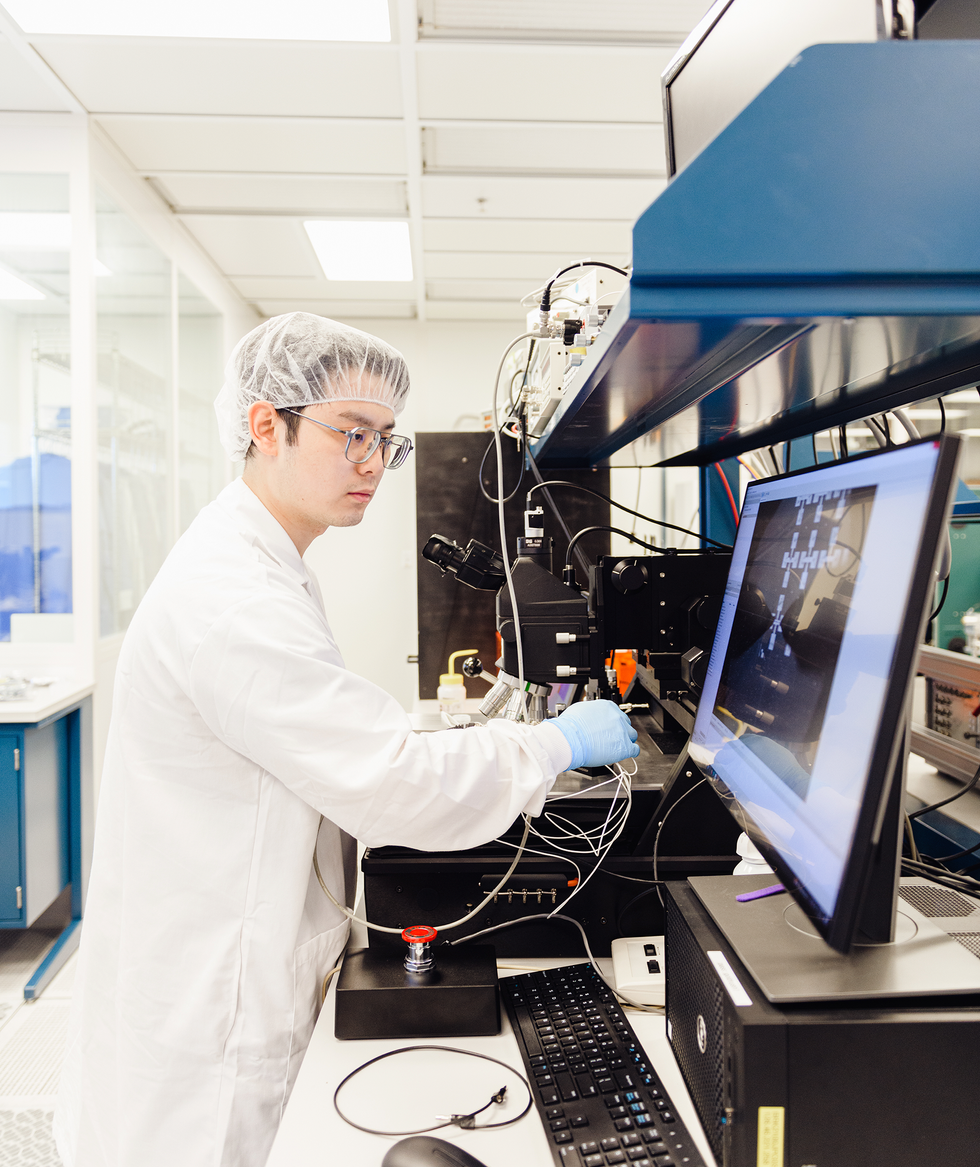 Graduate students Laura Chavez [top] and Marvin Zhang [above] use Purdue University’s Brick Nanotechnology Center to characterize semiconductors and ICs. SkyWater, a Minnesota-based foundry, is building a fab near the university. Top: Charles Jischke/Purdue University; Bottom: Rebecca Robiños/Purdue University
About 400 kilometers (250 miles) west of Intel’s development, another fab is planned. In July 2022, SkyWater Technology, a foundry that makes chips using specialty and mature manufacturing processes, announced a $1.8 billion chip fab at an industrial park in West Lafayette, Ind. Next door, Purdue has launched a new interdisciplinary Semiconductor Degrees Program to give undergraduate and graduate students a range of options for gaining core skills needed for the semiconductor industry. While EE courses traditionally cover integrated circuits and chip design, the new program teaches other key chip-manufacturing steps, including chemicals, materials, tools, manufacturing, packaging, and even supply-chain management. Students can choose to minor in the program, earn a master’s degree, or get a certification.
SkyWater representatives will inform students about various career options in the program’s introductory seminar course. Students are guaranteed experience in Purdue’s nanotechnology centers and at semiconductor companies. Advanced courses cover semiconductor materials and devices, as well as industrially relevant system-on-chip design. The program builds on Purdue’s SCALE program, funded by the U.S. Department of Defense and launched in 2020, which trains undergrads to design and build semiconductors for space. “SCALE is specific to defense microelectronics, but the SCALE and semiconductor-degrees programs are synergistic,” says Purdue’s Bermel. “Chips are fairly agnostic in many ways about the exact application space.”
This year, Purdue will kick off a new program aimed at educating workers for SkyWater. Supported by state and regional economic-development organizations, the program will include operator and technician training through associate degree courses at partner Ivy Tech Community College. Besides developing targeted coursework and internships with the company, the Purdue team plans outreach at local high schools about job opportunities at their neighboring fab, with the hopes of attracting more students to engineering.
A summer internship at SkyWater’s Florida foundry solidified Purdue undergraduate Anika Bhoopalam’s interest in the semiconductor industry. Bhoopalam, a senior majoring in chemical engineering with a minor in electrical and computer engineering, feels that the physics, materials science, and engineering courses she has taken, combined with research lab experience fabricating thin films and solar cells, have prepared her well. She plans to pursue a Ph.D. with a focus on materials science and solid-state physics so she can go on to work in chip manufacturing. “I found the semiconductor industry to be a fast-paced, exciting, and interesting field where you get to work on different tasks every day.”
Illinois ups its chip education game
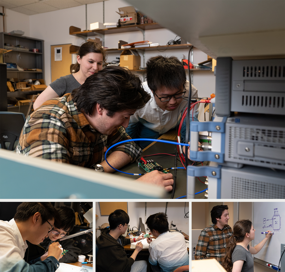 Undergraduate engineering students at the University of Illinois Urbana-Champaign take part in a course on designing and constructing ICs, which was once considered graduate-level work. Here, Jenna Cario [gray shirt], Andy Ng [plaid], Stanley Wu [white and blue] and Curtis Yu [in black] collaborate on various projects.
Virgil Ward/University of Illinois Urbana-Champaign
Students traditionally develop, build, and test integrated circuits in graduate school. But universities are trying to provide that first hands-on experience earlier. In the fall of 2021, electrical and computer engineering professors Pavan Hanumolu and Rakesh Kumar at the University of Illinois Urbana-Champaign created a class called Advanced Systems Design, which leads senior-year undergrads through every step of making an integrated circuit.
“It’s a nitty-gritty job,” says Hanumolu. “Companies don’t want students learning this on the job. If we can provide these skills, that might shorten the route to increasing the talent pool for industry.”
Students work in teams, defining a problem and designing a functional CMOS integrated circuit to solve it. The designs are sent off to a TSMC fab for manufacture, after which students test the chips, redesign the circuit as needed, and create a printed circuit board for the chip. So far, 30 students have taken the class, Kumar says, and several have gone on to internships and jobs with companies like Apple, Intel, and Siemens. “Employers have appreciated the rigor our students go through,” Hanumolu says. “They know the kind of unique skill set these students will graduate with.”
Arizona State adds TSMC
 Staff member Alex Cabrera [left] and student Monica Gaytan walk through a lab at the MacroTechnology Works research facility, where Arizona State University students work with fab equipment. Deanna Dent/Arizona State University
While cutting-edge chip fabs might be new in the Midwest, in the Southwest, Arizona State University has had a head start in preparing for an expanding onshore chip industry. Motorola picked the deserts near Phoenix for its plant back in the 1960s. Aerospace and defense companies followed, and then Intel arrived in the 1980s and is currently expanding. Most recently, TSMC broke ground on its big U.S. fab complex in Phoenix in 2021. Connections to the companies form a solid foundation for semiconductor education and research at ASU, says Kyle Squires, dean of the engineering school.
“You can see in our DNA the origins from this semiconductor presence going back to the ’60s,” he says. A significant fraction of the EE faculty comes in with industry experience and has close ties with industry. They bring their expertise into the hardware engineering classes and labs they design, Squires says, while giving students access to scholarships, research opportunities, internships, and eventually jobs. “It’s a way for us to maintain currency with these companies, what they’re doing, where they’re headed. As technology needs continue to move, so does the curriculum. It’s research informing teaching, and vice versa. It’s a feedback loop.”
ASU boasts a large microelectronics facility—originally a Motorola semiconductor fab—and EE students in their junior and senior years can choose electives that give them direct semiconductor processing experience in the facility’s clean rooms. Graduate students, meanwhile, can pursue a 15-credit Certificate in Semiconductor Processing that trains them in various aspects of chip production. Squires acknowledges that putting multimillion-dollar tools into an undergrad lab is unrealistic for most universities, so forging relationships with industry partners can help make up the difference.
Community colleges could be key
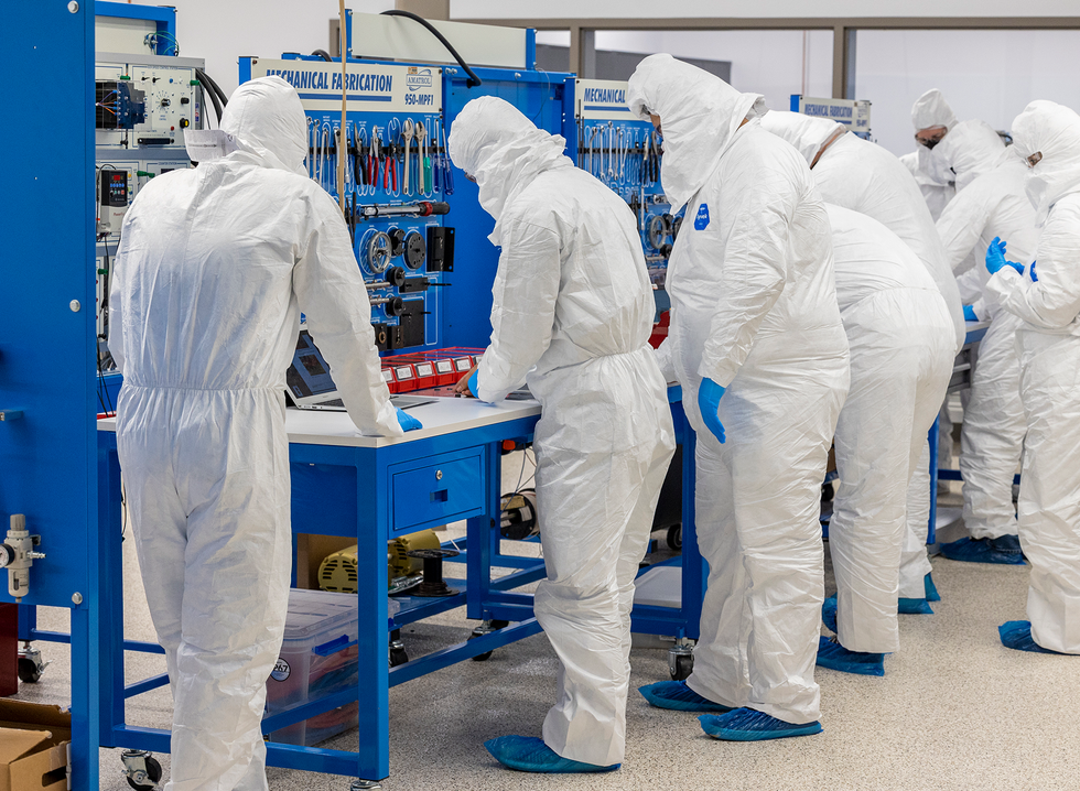 Community colleges will be key to filling the workforce needs of new fabs. Here, Maricopa Community College students work in an Intel-sponsored lab in Tempe, Ariz.Maricopa Community College/Intel
More than being a partner, Intel sees itself as a catalyst for upgrading the higher-education system to produce the workforce it needs, says the company’s director of university research collaboration, Gabriela Cruz Thompson. One of the few semiconductor companies still producing most of its wafers in the United States, Intel is expanding its fabs in Arizona, New Mexico, and Oregon. Of the 7,000 jobs created as a result, about 40 percent will be for people with two-year degrees, and 20 percent each for those with bachelor’s degrees, master’s degrees, and Ph.D.s.
Since COVID, however, Intel has struggled to find enough operators and technicians with two-year degrees to keep the foundries running. This makes community colleges a crucial piece of the microelectronics workforce puzzle, Thompson says. In Ohio, the company is giving most of its educational funds to technical and community colleges so they can add semiconductor-specific training to existing advanced manufacturing programs. Intel is also asking universities to provide hands-on clean-room experience to community college students.
Samsung and Silicon Labs in Austin are similarly investing in neighboring community colleges and technical schools via scholarships, summer internships, and mentorship programs. Samsung supports an initiative at Austin Community College that provides technician training for high school students. The company’s Fab Apprentice Program, meanwhile, allows students to complete their associate degree while working at Samsung two days a week. “We pay 100 percent of tuition and books as long as the student maintains a 3.0 GPA or higher,” says Michele Glaze, head of communications and community affairs at Samsung Austin Semiconductor.
Workforce shortages everywhere
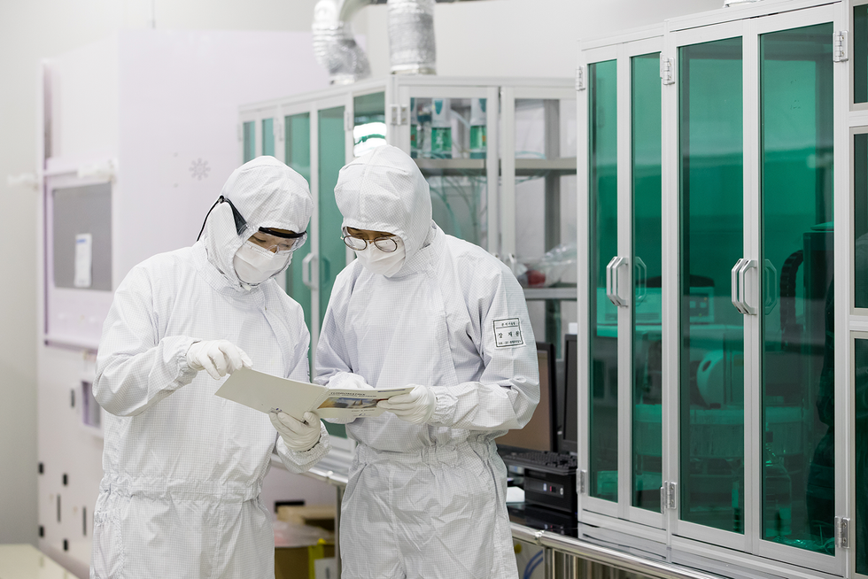 Chip companies are struggling to find workers in South Korea, too. Here, Samsung employees work on a project during their job-related training.Samsung
The semiconductor talent shortage isn’t unique to U.S. shores. Taiwan makes about 65 percent of the world’s chips, but finding young semiconductor engineers has been getting difficult, according to reports. Semiconductor firms around the world are competing for talent: They’re hiking salaries and doling out scholarships, internships, and mentorships to undergraduates and even vocational high school students, in hopes of attracting them early. “As the need for advanced semiconductors continues to increase and chip manufacturers compete for talent, we see the supply in the workforce trailing the high demand,” Samsung’s Glaze says.
Samsung works with four major universities in South Korea, providing tailored curricula to train students in semiconductor R&D and manufacturing. Taiwan’s government, meanwhile, is partnering with chip companies to invest $300 million in specialized chip-focused graduate schools within top universities to train the next generation of semiconductor engineers.
Enticing more students to study engineering is a big problem, Intel’s Thompson says. Attractive jobs in the software industry have led to a shift in the balance between electrical engineering and computer science. “We hear from academics that we’re losing EE students to software,” she says. “But we also need the software. I think it’s a totality of ‘We need more students in STEM careers.’”
The CHIPS Act might just be what was needed to put semiconductors in the limelight and entice students to hardware-related degrees. At Purdue, Bermel says he has seen an uptick in interest in the semiconductor information session at the annual September career fair. Historically, the fair has had a handful of semiconductor employers, but it had 28 this year and attracted over 600 students. For the semiconductor industry to be more successful going forward, the software industry’s practices might be worth following, he says. That includes “providing better opportunities for students even after only the first year of undergrad if possible, paying them very well, but also making it more evident to the general public why semiconductor companies are important.”
